
Internship with FermionIC

Designing a Phased Array Radar
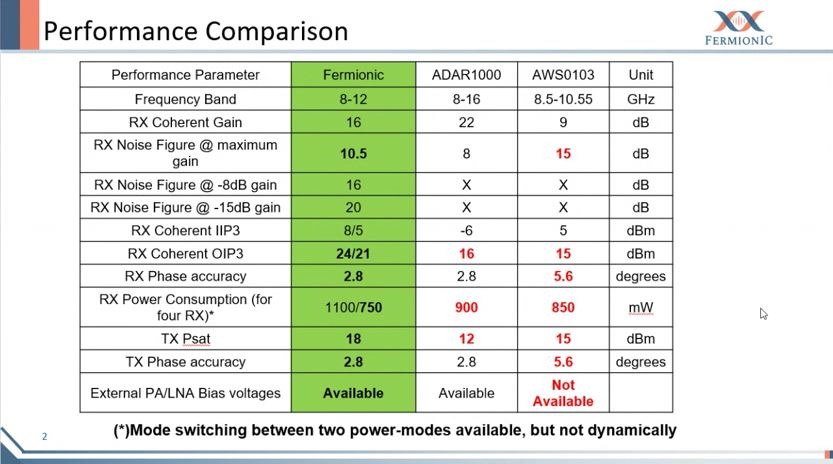
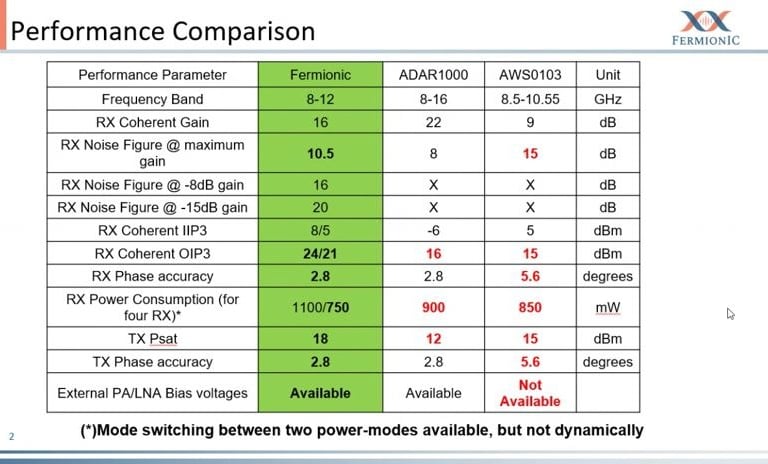
During my internship at FermionIC, I had the opportunity to work on the development of a phased array radar system, incorporating the ADAR1000 chip for beamforming applications. This project introduced me to advanced concepts in radar technology, RF engineering, and signal processing, deepening my understanding of modern communication systems. My primary focus was on the hardware design aspect, where I explored the intricacies of half-duplex and full-duplex radar systems, the role of quad TRM (Transmit-Receive Module) radios, and how X-Band phased array radar technology operates
To strengthen my theoretical foundation, I watched multiple technical webinars, including those from Analog Devices, and studied Jon Kraft’s video lectures on phased array radar principles and signal processing. These resources helped me grasp key concepts such as electronic beam steering, antenna array design and signal phase manipulation, which are critical to the functioning of phased array radars. I also researched the differences between half-duplex and full-duplex systems, particularly how their antenna configurations influence transmission and reception capabilities.
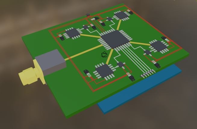
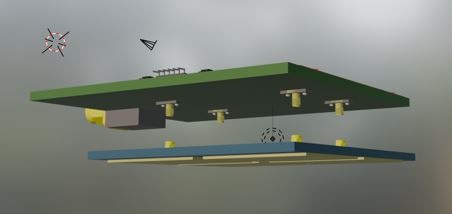
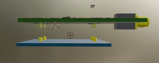
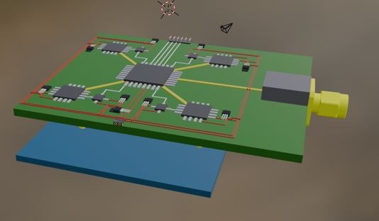
For the hands-on aspect of the project, I was tasked with designing a 3D model of the radar system, which I created using Blender due to its versatility in mechanical modeling. My design incorporated key components such as the FD3R4400A beamformer chip and FEM10W PA/LNA switcher chips, with a compact 4-channel SMA-based antenna array. In refining the model, I paid special attention to power input, control lines, GPIO placement, voltage regulation, and electromagnetic shielding to ensure an efficient and practical design.
Throughout this process, I collaborated closely with engineers at FermionIC, including the CTO, Mr. Prasun, who reviewed my design and provided valuable insights. After discussing my initial model, I was asked to make enhancements, including adding a daughterboard with a phased array antenna, integrating Mini SMA plugs to all PA/LNA switcher chips, and implementing coplanar transmission lines for improved signal integrity. I also researched 3D modeling tools for circuit design, such as SolidWorks and Altium, to expand my skill set in PCB layout and RF circuit design.
Currently, I am awaiting schematic details for the FEM LNA+PA chip, which will allow me to finalize the design and move toward potential prototyping. This project has been a transformative experience, reinforcing my passion for RF technology, radar systems, and hardware innovation. I am excited to continue exploring advancements in semiconductor-based communication and defense technologies, aiming to contribute to the future of high-performance radar and wireless systems.




xSpace.Space - Yash Xavier's Digital Space
Explore my Journey
My Personal Pursuits
© 2026. All rights reserved.
Showcase of Endeavour
Projects & Achievements
